
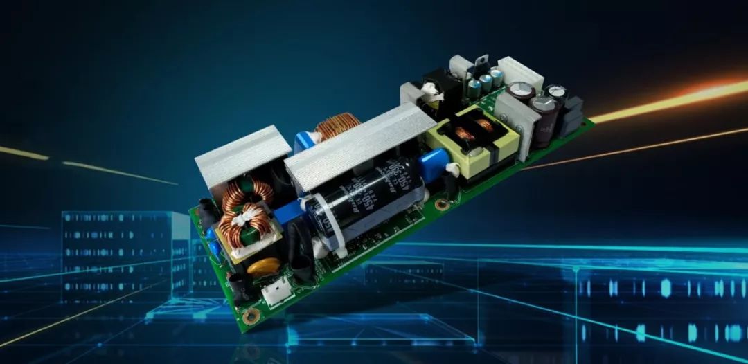
The design of the power supply is very important in the embedded industry, communication industry and industrial control industry, and the reliable and stable power supply scheme can make the product work more stable, better performance and longer working life.
In the process of PCB design, from the EMC point of view, three main factors must first be considered: input/output parameters, device density and power consumption. A practical rule is that the area of the chip element is 20% of the substrate, and the power dissipation per square inch is no more than 2W. In terms of device layout, in principle, the devices related to each other should be as close as possible, the digital circuit, the analog circuit and the power circuit are placed separately, and the high-frequency circuit and the low-frequency circuit are separated. Devices that are easy to produce noise, small current circuits, large current circuits, etc. should be kept away from logic circuits as far as possible. Major interference and radiation sources such as clock circuits and high-frequency circuits should be arranged separately, away from sensitive circuits. The I/O chip should be located near the I/O outlet of the hybrid circuit package.

In the process of PCB design, from the EMC point of view, three main factors must first be considered: input/output parameters, device density and power consumption. A practical rule is that the area of the chip element is 20% of the substrate, and the power dissipation per square inch is no more than 2W. In terms of device layout, in principle, the devices related to each other should be as close as possible, the digital circuit, the analog circuit and the power circuit are placed separately, and the high-frequency circuit and the low-frequency circuit are separated. Devices that are easy to produce noise, small current circuits, large current circuits, etc. should be kept away from logic circuits as far as possible. Major interference and radiation sources such as clock circuits and high-frequency circuits should be arranged separately, away from sensitive circuits. The I/O chip should be located near the I/O outlet of the hybrid circuit package.
(3) The wiring layer should be arranged as close as possible to the power supply or ground plane to produce flux cancellation.
There are three manufacturing processes available for hybrid integrated circuits: single layer film, multi-layer thick film and multi-layer co-fired thick film. Thin film process can produce the small size, low power and high current density components required for high-density hybrid circuits, with high quality, stability, reliability and flexibility, suitable for high-speed high-frequency and high package density circuits. However, it can only do single-layer wiring and the cost is high.
Multilayer thick film technology can manufacture multilayer interconnect circuits at a lower cost. From the perspective of electromagnetic compatibility, multilayer wiring can reduce the electromagnetic radiation of the circuit board and improve the anti-interference ability of the circuit board. Because special power layers and strata can be set up, the distance between the signal and the ground wire is only the interlayer distance. In this way, the loop area of all signals on the board can be reduced to a minimum, thus effectively reducing the differential mode radiation. The multi-layer co-fired thick film process has more advantages and is the mainstream technology of passive integration at present. It can realize more layers of wiring, easy to embed components, improve assembly density, and has good high-frequency characteristics and high-speed transmission characteristics.
In addition, it has good compatibility with thin film technology, and the combination of the two can achieve hybrid multilayer circuits with higher assembly density and better performance. The active device in the hybrid circuit generally uses the bare chip, and the corresponding packaged chip can be used when there is no bare chip. In order to obtain the best EMC characteristics, the surface mount chip is selected as far as possible. When selecting a chip, try to choose a low speed clock under the premise of meeting the technical specifications of the product. Never use AC when HC can be used, and CMOS4000 can do without HC. The capacitor should have a low equivalent series resistance, which can avoid large attenuation of the signal.